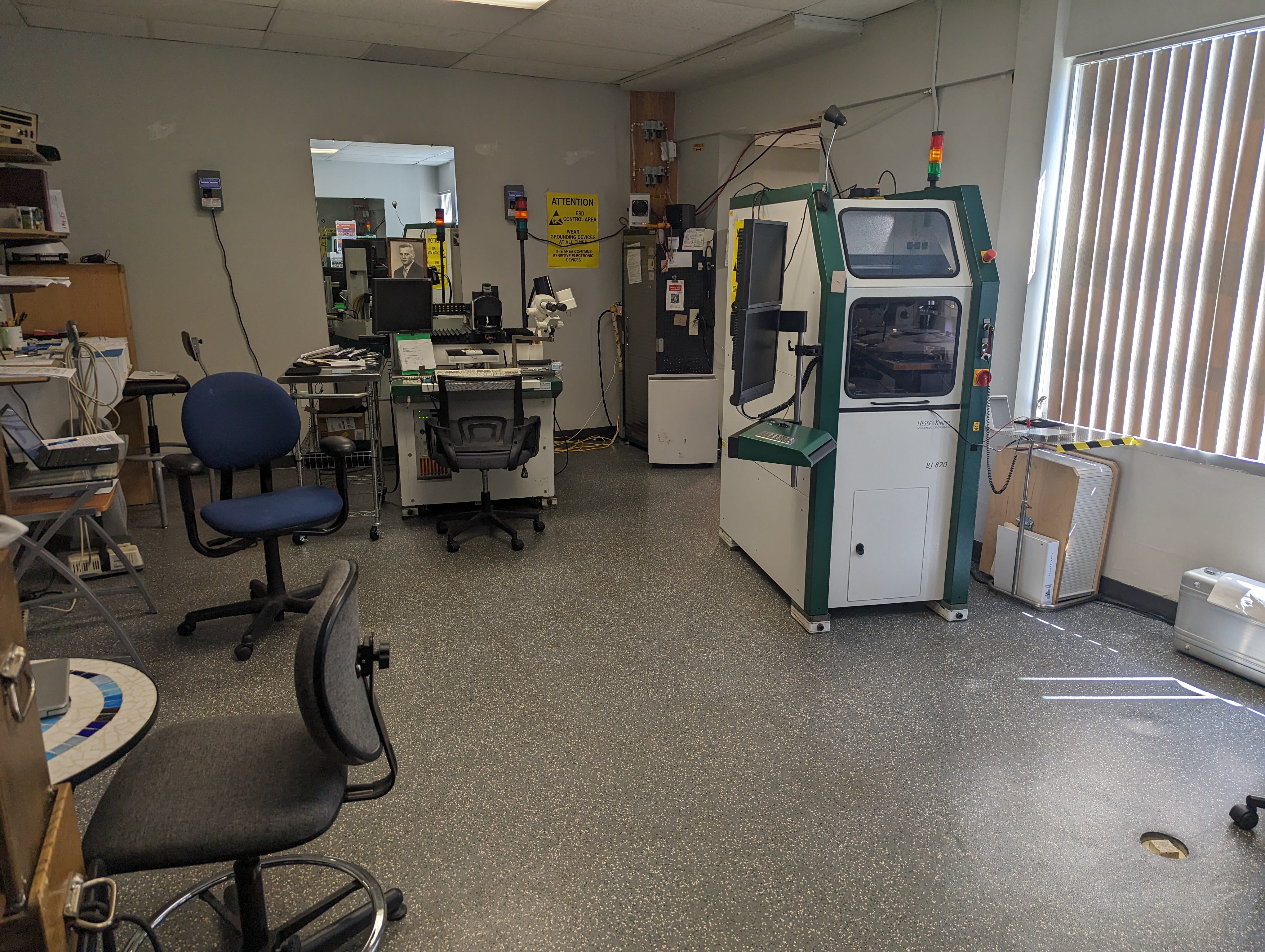
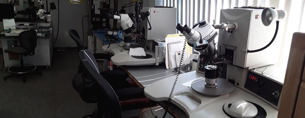
Our current customers utilize standard Kyocera side brazed DIP packages of different pin counts, materials, and well sizes based on chip dicing parameters. Our bonding systems are versatile and will accept a variety of die packages allowing us to participate in many different sectors of the industry. We die attach using high temperature RTV or epoxies. Coupled with another qualified vendor in New York, each with over 30 years of experience in the industry of packaging chip technologies, we can dice wafers of different diameters.
Connecting semiconductors and people through the same wire is what we do. Our work goes well beyond the bonder, connecting a circuit to an interface using very fine wire. We connect technologies for different processes or applications in communication, distance learning, medical, internet of things, cellular systems, and handsets for first responders. It is all connected, from the start of the process build, to bonding, stress and test, on to the application. Wire bonding is an integral part of connectivity for testing, functionality and application of today’s high-tech processes.

Semi-Conn NE’s principal owner, Tom Jones, has worked in the industry for over 40 years. He was employed at IBM’s East Fishkill, New York, lab for 35 years, then at Global Foundries for 5-plus years. Tom also served four years in the Marine Corps traveling the globe, working on avionics on helicopters, and developing a sense of esprit de corps, discipline, and loyalty. A graduate of Marist College in Poughkeepsie, New York, Tom earned a Bachelor of Science degree in Technology Management. With a keen focus on customer goals, Tom leads Semi-Conn NE forward with a commitment to excellence in communication, loyalty, and flexibility.


